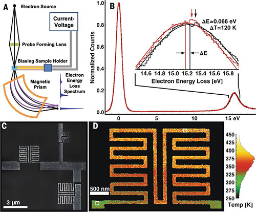
Temperature mapping on the nanoscale
Microelectronic devices can be simultaneously seen and tested with a biasing holder—taking advantage of the TEM’s analytical toolbox, like in this example, where the in-situ TEM biasing holder and EELS are used to capture changes in temperature. A team led by UCLA demonstrate a noncontact thermometric technique to measure bulk temperatures with nanometer-scale spatial resolution using plasmons.
Reference: B.C. Regan et al. Nanoscale temperature mapping in operating microelectronic devices. Science (2015). Abstract
Copyright © 2016 by the American Association for the Advancement of Science