| 1600 Series | |
| Tilt Range | ±45° depending on microscope and pole piece |
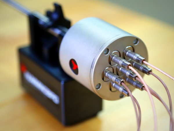
| Number of Electrical Contacts | 6, 8, or 9 * |
| Contact Type | Flexible wirebond contacts or fixed spring contact |
| Carrier | Removable Sample Carrier |
| Carrier Compatibility | Any Standard TEM Sample Supports |
| Sample Size | Fits up to 3 x 6mm samples |
| Wiring | Standard or low-noise shielded |
| TEM Compatibility | TFS/FEI, JEOL, Hitachi, Zeiss |
Overview
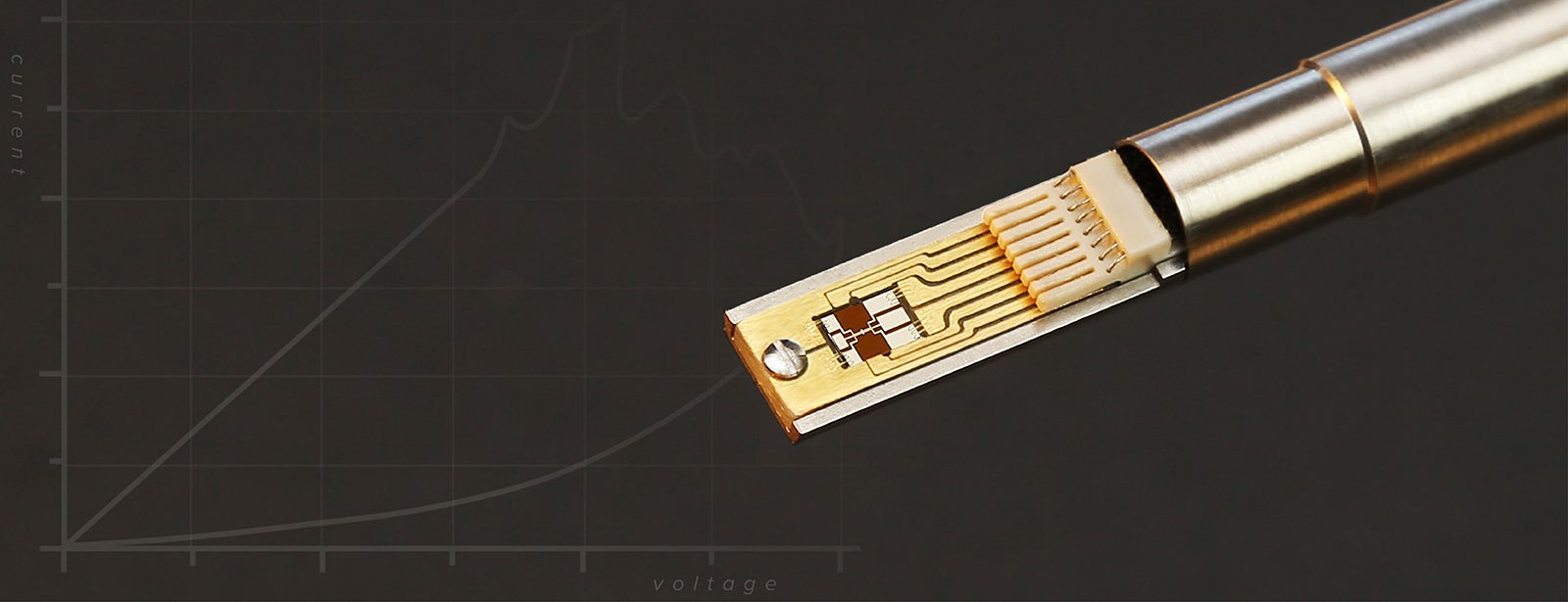
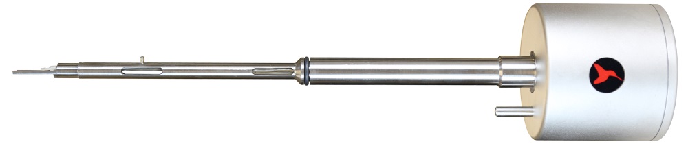
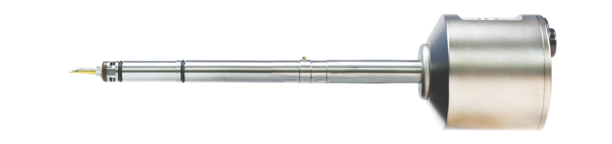
Hummingbird Scientific’s in-situ electrical biasing holder allows researchers to investigate the electrical response of materials inside the transmission electron microscope. The standard biasing holder has a removable chip carrier that accommodates a wide range of TEM sample geometries. This design allows convenient sample preparation outside the holder and is compatible with all of Hummingbird Scientific’s membrane substrates. Low-noise wiring ensures accurate measurements.
Sample Applications
- Correlating the electrical properties of nanoscale material and microstructures
- Studying the relationship between material defect populations and electrical responses
- Electromigration studies
- Operating microelectomechanical systems (MEMS) based mechanical testing devices
- In-situ testing of solid-state energy devices
|
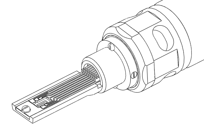
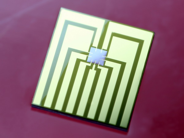
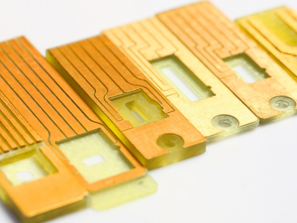
Board ContactThis contact configuration features a removable, reusable sample carrier which allows researchers to prepare the sample directly on the board. |
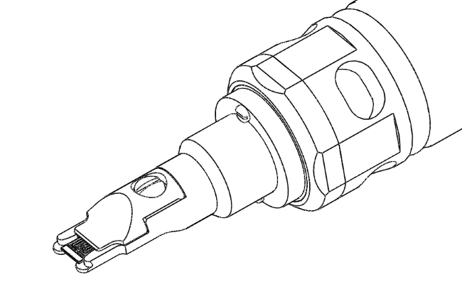 |
Direct Chip ContactThis contact configuration features a single chip that is directly inserted into the holder via a proprietary connector with up to 9 electrical contacts. |

Options
The 1600-series holder features a range of special options:
- Custom-designed sample carriers to fit almost any TEM sample geometry
- Low-noise, individually-shielded cabling option for pA-range current measurements.
- Keithley 2400 SMU
Related Products
Biasing Manipulator HolderSee MoreOn-site electrical contacts with mobile probe |
|
MEMS Biasing + Heating HolderSee MoreHigh temperature transport measurements—phase changes |
|
 |
Cryo-Biasing Holder See MoreElectrical biasing of cryo-cooled samples |
Air-Free Transfer Biasing Holder See MoreAir-free sample transfer to the TEM |
Edit
Temperature mapping on the nanoscale
Microelectronic devices can be simultaneously seen and tested with a biasing holder—taking advantage of the TEM’s analytical toolbox, like in this example, where the in-situ TEM biasing holder and EELS are used to capture changes in temperature. A team led by UCLA demonstrate a noncontact thermometric technique to measure bulk temperatures with nanometer-scale spatial resolution using plasmons.
Reference: B.C. Regan et al. Nanoscale temperature mapping in operating microelectronic devices. Science (2015). Abstract
Copyright © 2016 by the American Association for the Advancement of Science
Edit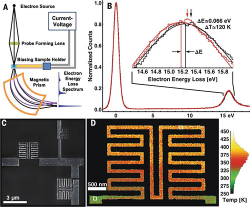
Joule heating and EELS spectrum of Al device. Image copyright © 2016 by the American Association for the Advancement of Science
Using our electrical biasing holder, researchers at Penn State have demonstrated the room temperature dislocation-based plasticity and tremendous flaw tolerance of TiN film, which in bulk form is a brittle material. TiN loading was conducted using a MEMS device containing electro-thermal actuators. The researchers surmise that room-temperature dislocation activities resulted from the nucleation of pre-existing dislocations, which resulted from residual compressive stresses developed during deposition. As a result, the TiN films were tougher than the Ti films in the tested multilayers. The movie shows the dislocation movement at the crack tip following loading at room temperature.
Reference: S. Kumar, D.E. Wolfe, M.A Haque. “Dislocation shielding and flaw tolerance in titanium nitride,” International Journal of Plasticity 27:5 (2011) pp. 739–747 . Abstract
Movie copyright © 2010, Elsevier Ltd. All rights reserved.
Edit


| Thomas R. Koenig, Hongyu Wang, Yong Zhu, Ankit Gupta, Garritt J. Tucker, and Gregory B. Thompson. “In situ characterization of thermomechanically loaded solution strengthened, nanocrystalline nickel alloys,” Acta Materialia (2024) | Abstract |
| Sandra Stangebye, Xing Liu, Lina Daza Llanos, Yichen Yang, Ting Zhu, Josh Kacher, Olivier Pierron. “Comparison of electrical sensing and image analysis for in situ transmission electron microscopy nanomechanical testing of thin films,” Thin Solid Films (2023) | Abstract |
| Jared J. Lodico, Matthew Mecklenburg, Ho Leung Chan, Yueyun Chen, Xin Yi Ling, and B. C. Regan. “Operando spectral imaging of the lithium ion battery’s solid-electrolyte interphase,” Sci. Adv. (2023) | Abstract |
| Oscar Recalde-Benitez, Tianshu Jiang, Robert Winkler, Yating Ruan, Alexander Zintler, Esmaeil Adabifiroozjaei, Alexey Arzumanov, William A. Hubbard, Tijn van Omme, Yevheniy Pivak, Hector H. Perez-Garza, B. C. Regan, Lambert Alff, Philipp Komissinskiy, and Leopoldo Molina-Luna. “Operando two-terminal devices inside a transmission electron microscope,” Commun. Eng. (2023) | Abstract |
| William A. Hubbard, Jared J. Lodico, Ho Leung Chan, Matthew Mecklenburg, and B. C. Regan. “Nanoscale Conductivity Mapping: Live Imaging of Dielectric Breakdown with STEM EBIC,” IEEE International Symposium on the Physical and Failure Analysis of Integrated Circuits (IPFA) (2022) | Abstract |
| William A. Hubbard, Jared J. Lodico, Xin Yi Ling, Brian T. Zutter, Young-Sang Yu, David A. Shapiro, B.C. Regan. “Differential electron yield imaging with STXM,” Ultramicroscopy (2021) | Abstract |
| William A. Hubbard, Jared J. Lodico, Ho Leung Chan, Matthew Mecklenburg, and Brian C. Regan. “Imaging Dielectric Breakdown in Valence Change Memory,” Advanced Functional Materials (2021) | Abstract |
| Thomas Koenig, Hongyu Wang, Kayla Cole-Piepke, Alicia Koenig, Sourav Garg, Garritt Tucker, Patrick Kung, Tim Mewes, Claudia Mewes, John Nogan, Yong Zhu, and Gregory Thompson. “In Situ Thermomechanical Loading for TEM Studies of Nanocrystalline Alloys,” Microscopy and Microanalysis (2021) | Abstract |
| Saurabh Gupta, Sandra Stangebye, Katherine Jungjohann, Brad Boyce, Ting Zhu, Josh Kachera, and Olivier N. Pierron. “In situ TEM measurement of activation volume in ultrafine grained gold,” Nanoscale (2020) | Abstract |
| William A. Hubbard, Matthew Mecklenburg, Jared J. Lodico, Yueyun Chen, Xin Yi Ling, Roshni Patil, W. Andrew Kessel, Graydon J. K. Flatt, Ho Leung Chan, Bozo Vareskic, Gurleen Bal, Brian Zutter, and B. C. Regan. “Electron-Transparent Thermoelectric Coolers Demonstrated with Nanoparticle and Condensation Thermometry,” ACS Nano (2020) | Abstract |
| Paul Masih Das and Marija Drndić, “In Situ 2D MoS2 Field-Effect Transistors with an Electron Beam Gate,” ACS Nano (2020) | Abstract |
| June W. Lau, Karl B. Schliep, Michael B. Katz, Vikrant J. Gokhale, Jason J. Gorman, Chunguang Jing, Ao Liu, Yubin Zhao, Eric Montgomery, Hyeokmin Choe, Wade Rush, Alexei Kanareykin, Xuewen Fu, and Yimei Zhu, “Laser-free GHz stroboscopic transmission electron microscope: Components, system integration, and practical considerations for pump–probe measurements,” Review of Scientific Instruments (2020) | Abstract |
| Brian Zutter, Hyunseok Kim, William Hubbard, Dingkun Ren, Matthew Mecklenburg, Diana Huffaker, and B. C. Regan. Mapping Charge Recombination and the Effect of Point Defect Insertion in Gallium Arsenide Nanowire Heterojunctions., arXiv:2010.05140 (2020) | Abstract |
| M. Mecklenburg, W. Hubbard, J. Lodico, and B.C. Regan. “Electron beam-induced current imaging with two-angstrom resolution,” Ultramicroscopy (2019) | Abstract |
| W. Hubbard, Z. Lingley, J. Theiss, S. Sitzman, T. Ayvazian, M. Brodie, and B. Foran. “Scanning transmission electron microscope mapping of electronic transport in polycrystalline BaTiO3 ceramic capacitors, Applied Physics Letters (2019) | Abstract |
| MJ. Lodico, M. Mecklenburg, H. Chan, W. Hubbard, and B.C. Regan. “STEM of a Single Crystal Lithium Ion Battery Anode during Electrochemical Cycling., Microscopy and Microanalysis (2019) | Abstract |
| W. Hubbard, J. Lodico, B. Zutter, D. Shapiro, Y. Lo, A. Rana, D. Morrill, C. Gentry, H. Chan, B.C. Regan. “Total Electron Yield Mapping of Electronic Devide Features via Measurement of X-Ray Beam Induced Currents,” Microscopy and Microanalysis (2019) | Abstract |
| Zahabul Islam, Aman Haque, and Nicholas Glavin, “Real-time visualization of GaN/AlGaN high electron mobility transistor failure at off-state,” Applied Physics Letters (2018) | Abstract |
| Jared J. Lodico, William A. Hubbard and B. C. Regan. “Scanning TEM Electron Beam Induced Current Imaging in Water.” Microscopy & Microanalysis (2018) | Abstract |
| Edward R. White, Jared J. Lodico & B. C. Regan. “Intercalation events visualized in single microcrystals of graphite,” Nature Communications (2017) | Abstract |
| Nathanael Jöhrmann, Steffen Hartmann, Kiran Jacob, Jens Bonitz, Kathrine E. MacArthur, Sascha Hermann, Stefan E. Schulz, Bernhard Wunderle. “A test device for in situ TEM investigations on failure behaviour of carbon nanotubes embedded in metals under tensile load,” 18th International Conference on Thermal, Mechanical and Multi-Physics Simulation and Experiments in Microelectronics and Microsystems (2017) | Abstract |
| J. Rodriguez-Manzo, Z. Qi, A. Crook, J. Ahn, A. Johnson, M.Drndic. “In Situ Transmission Electron Microscopy Modulation of Transport in Graphene Nanoribbons.” ACS Nano (2016) | Abstract |
| W. Parkin, A. Balan, L. Liang, P. Das, M. Lamparski, C. Naylor, J. Rodriguez-Manzo, A. Johnson, V. Meunier, M. Drndic. “Raman Shifts in Electron-Irradiated Monolayer MoS2.” ACS Nano (2016) | Abstract |
| J.J. Lodico, E.R. White, W.A. Hubbard, E. Garcia, B. Parks, B. Zutter, B.C. Regan. “In-Situ Scanning Transmission Electron Microscopy (STEM) of Individual Electrochemical Intercalation Events in Graphite,” Microscopy and Microanalysis (2015) | Abstract |
| M.L. Taheri. “Toward Deterministic Switching in Ferroelectric Systems: Insight Gained from In-Situ TEM,” Microscopy and Microanalysis (2015) | Abstract |
| M.-S. Hsiao, Y. Yuan, C. Grabowski, A. Nie, R. Shabazian-Yassar, L.F. Drummy. “In-Situ TEM Characterization of Nanostructured Dielectrics,” Microscopy and Microanalysis (2015) | Abstract |
| J. Hart, M. Jablonski, A. Lang, A. Damadoran, S. Liu, M. Arredondo, L. Martin, A. Rappe, M.L. Taheri.”Toward Deterministic Switching in Ferroelectric Systems: Insight Gained from In Situ TEM,”Microscopy and Microanalysis (2015) | Abstract |
| W.A. Hubbard, E.R. White, A. Kerelsky, G. Jasmin, J. Lodico. “Time-Resolved Imaging of Electrochemical Switching in Nanoscale Resistive Memory Elements,” Microscopy and Microanalysis (2015) | Abstract |
| B.C. Regan, W.A. Hubbard, E.R. White, R. Dhall, S.B. Cronin, S. Aloni, M. Mecklenburg. “Introduction to Plasmon Energy Expansion Thermometry,” Microscopy and Microanalysis (2015) | Abstract |
| M.H. Mecklenburg, W.A. Hubbard, E.R. White, R. Dhall, S. Cronin, S. Aloni, B.C. Regan. “Applications of Plasmon Energy Expansion Thermometry,” Microscopy and Microanalysis (2015) | Abstract |
| M. Mecklenburg, W. A. Hubbard,E. R. White, Rohan Dhall, S. B. Cronin, S. Aloni, and B. C. Regan“Nanoscale temperature mapping in operating microelectronic devices “, Science (2015) | Abstract |
| M. Puster, J.A. Rodríguez-Manzo, A. Balan, M. Drndić. “Toward Sensitive Graphene Nanoribbon-Nanopore Devices by Preventing Electron Beam-Induced Damage,” ACS Nano (2013) | Abstract |
| E. Hosseinan, O.N. Pierron, “Quantitative in situ TEM tensile fatigue testing on nanocrystalline metallic ultrathin films,” Nanoscale (2013) | Abstract |
| C.R. Winkler, M.L. Jablonski, A.R. Damodaran, K. Jambunathan, L.W. Martin, M.L. Taheri. “Accessing Intermediate Ferroelectric Switching Regimes With Time-Resolved Transmission Electron Microscopy,” Journal of Applied Physics (2012) | Abstract |
| C.R. Winkler, A.R. Damodaran, J. Karthik, L.W. Martin, M.L. Taheri. “Direct Observation of Ferroelectric Domain Switching in Varying Electric Field Regimes Using In-Situ TEM,” Micron (2012) | Abstract |
| Y. Inayoshi, H. Minoda, Y. Arai, K. Nagayama. “Direct Observation of Biological Molecules in Liquid by Environmental Phase-Plate Transmission Electron Microscopy,” Micron (2012) | Abstract |
| S. Kumar, D.E. Wolfe, M.A. Haque. “Dislocation Shielding and Flaw Tolerance in Titanium Nitride,” International Journal of Plasticity (2011) | Abstract |
| S. Kumar, D. Zhuo, D.E. Wolfe, A. Eades, M.A. Haque. “Length-Scale Effects on Fracture of Multilayers,” Scripta Materialia (2010) | Abstract |
| C.M. Wang, W. Xu, J. Liu, D.W. Choi, B. Arey, L.V. Saraf, J.G. Zhang, Z.G. Yang, S. Thevuthasan, D.R. Baer, N. Salmon. “In-situ transmission electron microscopy and spectroscopy studies of interfaces in Li ion batteries: Challenges and opportunities,” Journal of Materials Research (2010) | Abstract |
| S. Kumar, M.A. Haque. “Fracture Testing of Nanoscale Thin Films inside the Transmission Electron Microscope,” International Journal of Applied Mechanics (2010) | Abstract |
| D.T. Schoen, S. Meister, H. Peng, C. Chan, Y. Yangb, Y. Cuia. “Phase transformations in one-dimensional materials: applications in electronics and energy sciences,” Journal of Materials Chemistry (2009) | Abstract |
| H. Minoda, K. Hatano, H. Yazawa. “Development of a surface conductivity measurement system for ultrahigh vacuum transmission electron microscope,” Review of Scientific Instruments (2009) | Abstract |
| S. Kumar, M.A. Haque, H. Gao. “Notch-Insensitive Fracture in Nanoscale Thin Films,” Applied Physics Letters (2009) | Abstract |
| S. Meister, D.T. Schoen, M.A. Topinka, A.M. Minor, Y. Cui. “Void Formation Induced Electrical Switching in Phase-Change Nanowires,”Nano Letters (2008) | Abstract |
| H. Peng, C. Xie, D.T. Schoen, and Y. Cui. “Large Anisotropy of Electrical Properties in Layer-Structured In2Se3 Nanowires,” Nano Letters (2008) | Abstract |
Read More