2D Materials
| Biasing Manipulator TEM | Heating + Biasing TEM | Biasing TEM | Furnace Heating TEM | ||
| Stimuli |
Electrical |  |
|
|
|
| Thermal |  |
|
|
|
|
| Mechanical | |
||||
| Imaging | Higher resolution and diffraction | |
|
|
|
| EDS/EELS compatibility | |
|
|
|
|
| In-situ imaging | |
|
|
|
|
| Pre- and post-mortem analysis | |
|
|
|
|
| Sample Type |
Standard grid | |
|
|
|
| FIB lift-out | |
|
|
||
| MEMS chip | |
|
|
||
Excellent Good ![]() N/A
N/A
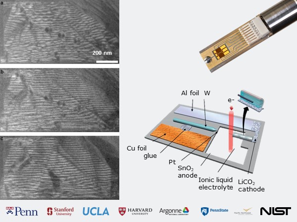
TEM Sample Holders for 2D Materials Research
Biasing Manipulator HolderSee MoreOn-site electrical contacts with mobile probe |
|
MEMS Biasing + Heating HolderSee MoreHigh temperature transport measurements—phase changes |
|
Biasing HolderSee MoreWire-bonded samples to investigate functional electrical devices |
|
Furnace Heating HolderSee MoreStandard bulk TEM samples at high temperatures |
2D Materials Electrochemistry
Hummingbird Scientific’s in-situ electrical biasing holder can be used for electrochemically cycling thin film batteries while imaging the material microstructure. Representative battery cell can be thinned using FIB processing or attached to the substrate. The sample is a representative section of the real battery cell and the data obtained is representative of the real battery performance.
For example, a thin cross-section of a battery cell can be mounted, wire-bonded, and viewed in TEM while cycling. The image shown on the left is a 10 nm graphite flake folded onto itself after one complete intercalation/deintercalation cycle.
Reference: Edward R. White, Jared J. Lodico & B. C. Regan. “Intercalation events visualized in single microcrystals of graphite,” Nature Communications (2017).
Image (left) © 2017 Macmillan Publishers Limited, part of Springer Nature
Image (bottom right) © Materials Research Society 2010
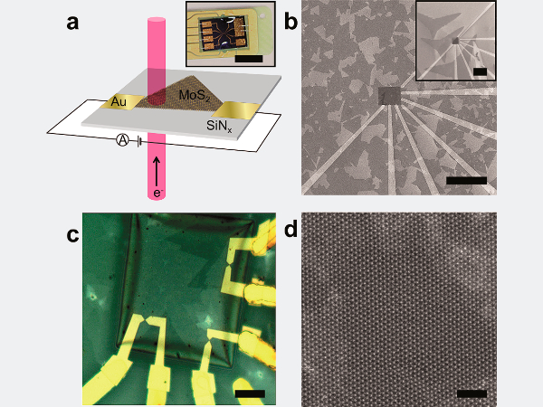
2D Materials-Based Devices
Two-dimensional materials-based electronic devices are particularly well suited for in-situ microscopy studies. Is relatively easy to contact continuous films and large crystals of 2D materials with Hummingbird Scientific’s biasing platforms. The example shown here illustrates that 2D materials-based devices suited for TEM studies can also be studied with other characterization techniques, in a correlative manner. Dr. Marija Drndić’s group at the University of Pennsylvania developed a process to study the effects of electron beam irradiation on one-atom-thick MoS2 crystals by combining in-situ TEM and ex-situ Raman spectroscopy data—from the same sample.
Reference: William M. Parkin et al. Raman Shifts in Electron-Irradiated Monolayer MoS2. ACS Nano (2016).
Image © 2014 American Chemical Society
Edit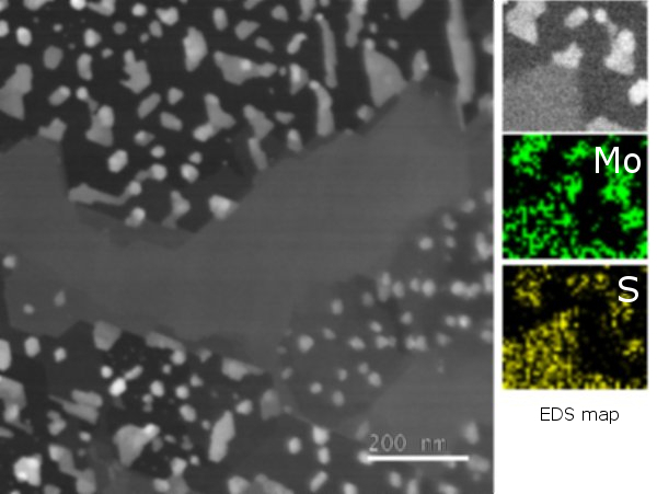
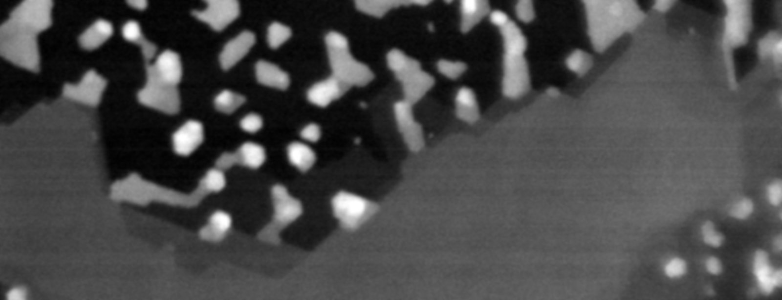
2D Materials at High Temperature
Hummingbird Scientific’s heating platforms allow researchers to heat 2D materials and—with some options—simultaneously apply voltages to the sample under observation. This example shows the segregation of MoS2 layers at high temperature. Researches at the University of Pennsylvania transformed few-layers of MoS2 with residual polymers from the transfer process into a 2D material with well segregated areas formed of either pure MoS2 or carbon based-composites. The segregation happens at temperature > 1000 °C. Energy-dispersive X-ray spectroscopy (EDS) confirmed the chemical content of each segregated area.
Data provided by Dr. Deep Jariwala and Dr. Eric Stach from the the University of Pennsylvania.
Edit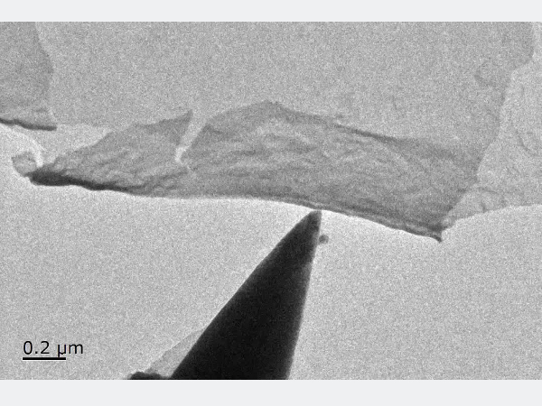
Biasing 2D Materials’ Edges
Hummingbird Scientific’s biasing-manipulator TEM holder’s movable biasing probe can be use to electrically contact 2D materials’ edges at specific locations with high spatial resolution. In this way, potential differences and electrical currents can be induced in the material locally. This examples shows a TEM image of contact between a metal probe of the biasing-manipulator TEM holder and the edge of a few-layers graphene sample.
Image courtesy of Dr. Yan Cheng from the Shanghai Institute of Microsystem and Information Technology.
EditTransport in Graphene Nanoribbons
In an electron microscope the electron beam’s main function is to act as an illumination source. However, in the right energy range the electron beam can displace atoms from a material. Marija Drndić’s group at the University of Pennsylvania developed a process to modify graphene sheets into graphene nanoribbons with the aid of a TEM’s electron beam. By having these modifications done in a Hummingbird Scientific in situ TEM biasing sample holder, the researchers were able to 1) fabricate graphene-based devices inside the TEM column and 2) characterize the devices electronically without the need to remove the sample from the microscope. This technique is well suited for any 2D material.
Reference: Marija Drndić et al. In Situ Transmission Electron Microscopy Modulation of Transport in Graphene Nanoribbons. ACS Nano (2016).
Edit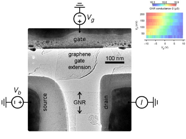 Image copyright © 2016 American Chemical Society
 | Edward R. White, Jared J. Lodico, and B. C. Regan. “Intercalation events visualized in single microcrystals of graphite,” Nature Communications (2017) | Abstract |
| William M. Parkin, Adrian Balan, Liangbo Liang, Paul Masih Das, Michael Lamparski, Carl H. Naylor, Julio A. Rodríguez-Manzo, A. T. Charlie Johnson, Vincent Meunier, and Marija Drndić. “Raman Shifts in Electron-Irradiated Monolayer MoS2,” ACS Nano (2016) |
Abstract |
| Julio A. Rodríguez-Manzo, Zhengqing John Qi, Alexander Crook, Jae-Hyuk Ahn, A. T. Charlie Johnson, and Marija Drndić. “In Situ Transmission Electron Microscopy Modulation of Transport in Graphene Nanoribbons,” ACS Nano (2016) | Abstract |
| Matthew Puster, Julio A. Rodríguez-Manzo, Adrian Balan, and Marija Drndić. “Toward Sensitive Graphene Nanoribbon-Nanopore Devices by Preventing Electron Beam-Induced Damage,” Small (2016) | Abstract |
| Matthew Puster, Adrian Balan, Julio A. Rodríguez-Manzo, Gopinath Danda, Jae-Hyuk Ahn, William Parkin, and Marija Drndić. “Cross-Talk Between Ionic and Nanoribbon Current Signals in Graphene Nanoribbon-Nanopore Sensors for Single-Molecule Detection,” Small (2015) | Abstract |
Read More