MEMS Heating + Biasing
| Single-Tilt | Double-Tilt | |
| Tilt Range | Up to ± 45° depending on objective pole | Up to ± 20° (alpha and beta) depending on objective pole |
| Beta-tilt accuracy | NA | <0.01 degree |
| Electrical Contacts | 9* | 9* |
| Contact Type | Direct Chip Contact | Direct Chip Contact |
| Max Operating Temperature | > 1000°C | > 1000°C |
| Settled Resolution at 1000°C | Up to TEM resolution | Up to TEM resolution |
| Temperature Stability | + 100 hours | + 100 hours |
| Temperature Measurement | 4-point resistance sensing | 4-point resistance sensing |
| Special cabling and sample carriers | High-voltage or High-frequency biasing | High-voltage or High-frequency biasing |
| EELS / EDS Compatible | Yes (full temp range) | Yes (full temp range) |
| TEM Compatibility | TFS/FEI, JEOL, Hitachi | TFS/FEI, JEOL, Hitachi |
Overview
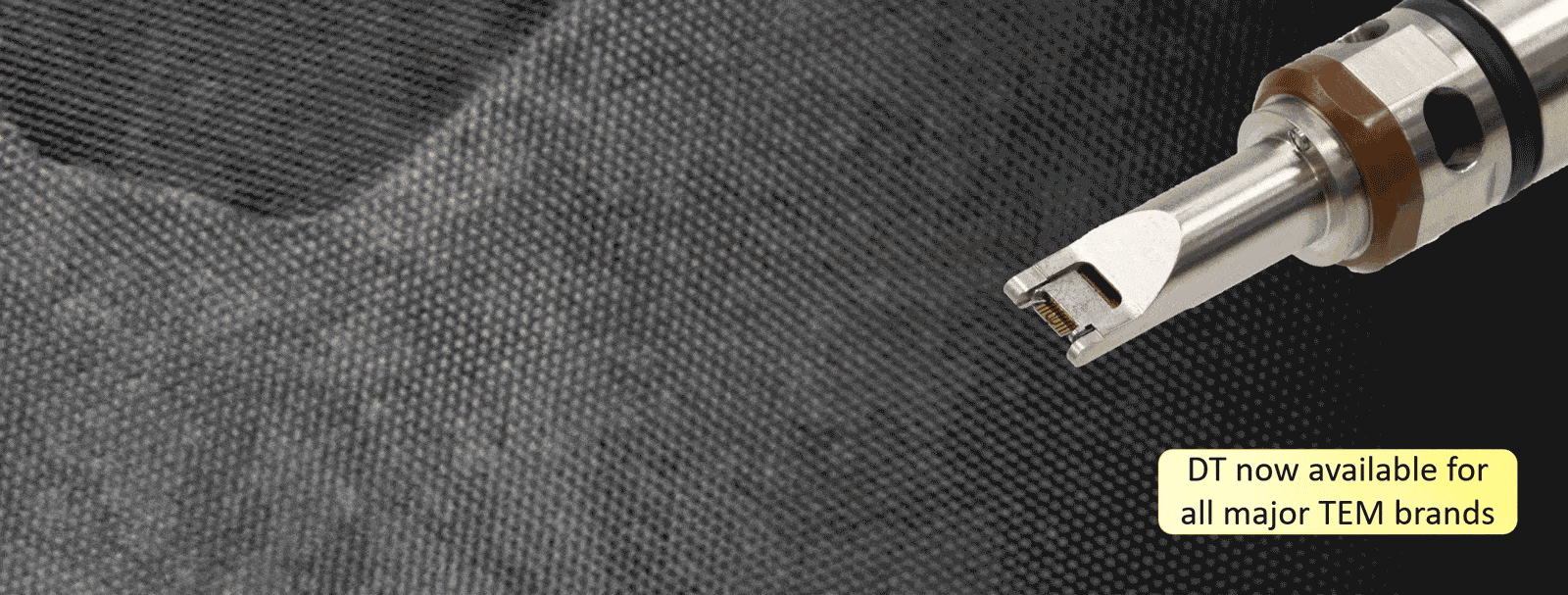
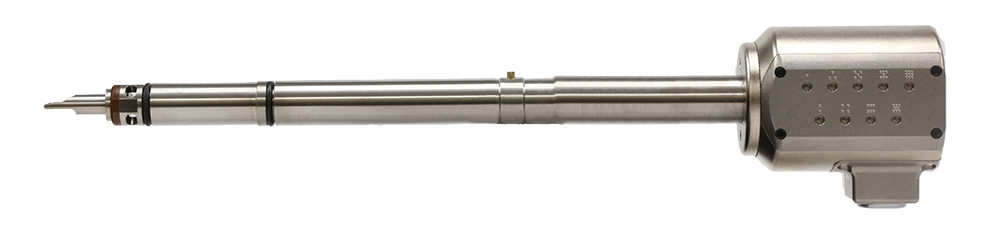
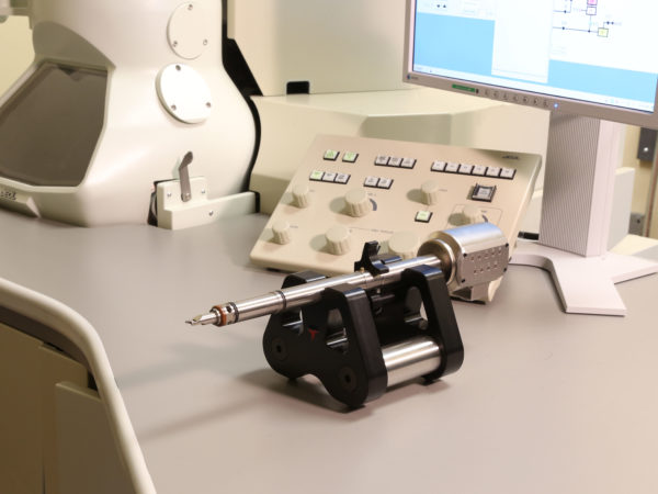
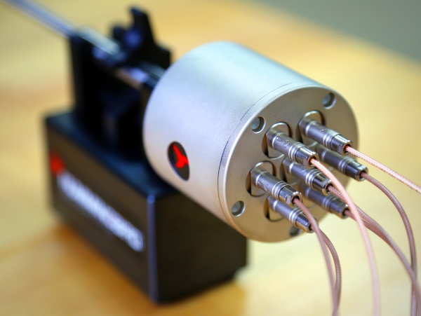
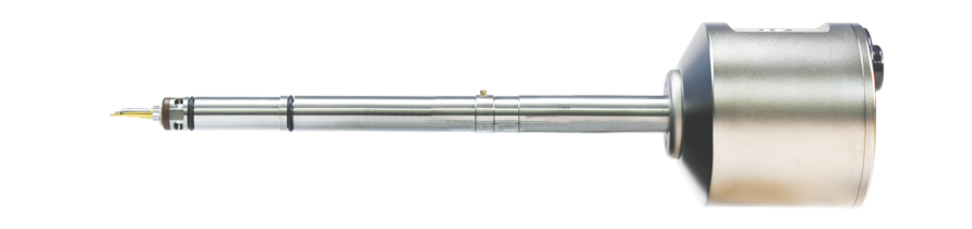
Hummingbird Scientific’s in-situ TEM MEMS Biasing/Heating Sample Holder allows users to heat and/or electrically bias their sample inside the TEM. Heating can be performed to > 1000°C in closed loop control with an on-chip sensor.
The system features:
- Direct chip contact insertion mechanism—no fragile probes that make inconsistent contact involved, so easy to use.
- Standard MEMS chip biasing/heating with 9 contacts
- Single and double tilt configurations
- 4-point temperature sensing method
- Shielded electrical cables for low current measurements
- Integrated heating and voltage source meter controller
- Intuitive graphical user interface for system control
- EDS compatible over the full temperature range
The system is available as a single-tilt and double-tilt version. The double-tilt holder features a high-accuracy (<0.01 degree) beta-tilt mechanism and no tilt-backlash when changing tilt direction, making it the most stable and usable double-tilt holder available.
Edit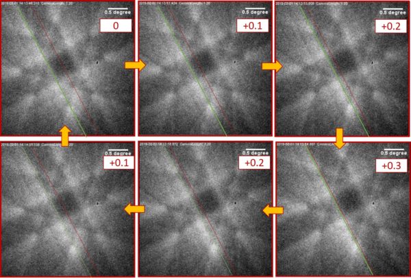
Accurate and repeatable beta-tilt
Accurate and repeatable beta-tilt
The beta-tilting resolution and accuracy of this double-tilt Heating + Biasing TEM holder are <0.01 degree. The negligible backlash one gets when reversing tilt direction that often makes other double-tilt TEM holders difficult to use is in the same order of magnitude.
The figure on the left shows beta-tilt from 0 to 0.3 to 0 degree with an exact return to 0.0 after tilting the same amount of steps in both directions.
Edit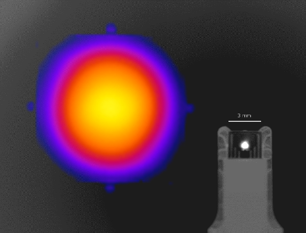
Heating
Hummingbird Scientific’s Heating + Biasing TEM holder platform is supported by our microfabrication team. All our MEMS chips are designed, fabricated, and tested in-house to assure optimal performance and quality.
Our fabricated MEMS chips-based microheaters provide:
- Temperatures > 1000°C
- 4-point resistance sensing
- > 100 hours of temperature stability
- Large field of view
- Compatibility with electron-based spectroscopy (EELS and EDS)
Learn more about our microfabrication facilities here.
Edit

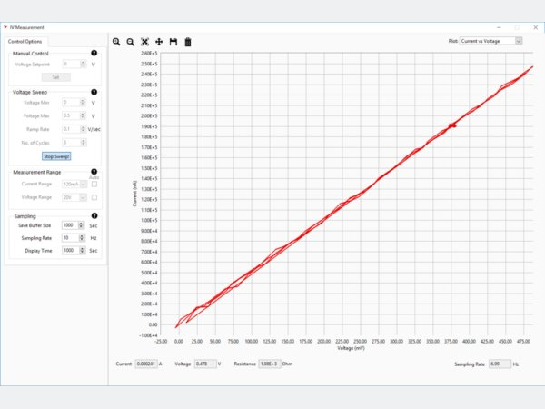
Biasing
Hummingbird’s Scientific Heating + Biasing sample holder has an industry leading 9 contacts (standard). All electrical contacts are available for non-heating biasing experiments with our biasing MEMS chips. While using the heating + biasing capability with our Heating-Biasing MEMS chips, four contacts are used for heating and sensing; the remaining five contacts are available for biasing the sample.
Hummingbird Scientific’s graphical user interface features intuitive controls for heating and biasing functions, including temperature-set point and voltage sweeps. Custom camera integration options are available.
All our MEMS chips are designed, fabricated, and tested in-house, and are available in our web store for our customers.
EditRelated Products
Biasing HolderSee MoreWire-bonded samples to investigate working devices |
|
Furnace HolderSee MoreStandard bulk TEM samples at high temperatures |
|
Biasing Manipulator HolderSee MoreOn-site electrical contacts with mobile probe |
|
 |
Cryo-Biasing Holder See MoreElectrical biasing of cryo-cooled samples |
Air-Free Transfer Biasing Holder See MoreAir-free sample transfer to the TEM |
Edit
Phase transformation of 2D transition metal (TM) dichalcogenides during the in-situ high-temperature heating
Two-dimensional (2D) TM dichalcogenides demonstrate exceptional electronic and optical properties. A previous study by researchers from the University of Pennsylvania on a few layers of 2D MoS2 has shown multiple phases with atoms occupying orientations within single/multiple layers (see npj 2D Materials and Applications here).
Here, the same group study different thin 2D dichalcogenide material and observe a unique conversion of phases from the parent crystalline substrate. The conversion is initiated when the temperature of the sample reaches around 500°C. The diffusion velocity of the new phase is dependent upon the stimulus applied to the sample.
Data provided by Pawan Kumar, Eric Stach and Deep Jariwala from the University of Pennsylvania.
Edit
In-situ TEM atomic scale diffusion between two quantum dots at high temperatures
The movie on the left shows atomic scale diffusion of atoms between two quantum dots heated to 650°C in-situ in the TEM using Hummingbird Scientific’s MEMS heating + biasing TEM sample holder. Atomic diffusion appears to occur mostly through the bridge between the two particles and continues until the two particles coalesce to form one larger particle.
Data provided by Pawan Kumar, Deep Jariwala and Eric Stach from the University of Pennsylvania.
Edit 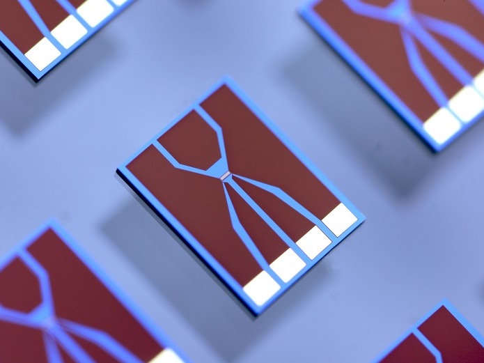

| Leifeng Zhang, Frédéric Lorut, Kilian Gruel, Martin J. Hÿtch, and Christophe Gatel. “Measuring electrical resistivity at the nanoscale in phase change materials,” Nano Lett. (2024) | Abstract |
| Gaurav Modi, Andrew C. Meng, Srinivasan Rajagopalan, Rangarajan Thiruvengadam, Peter K. Davies, Eric A. Stach, and Ritesh Agarwal. “Controlled self-assembly of nanoscale superstructures in phase-change Ge-Sb-Te nanowires” Nano Lett. (2024) | Abstract |
| Michael J. Motala, Xiang Zhang, Pawan Kumar, Eliezer F. Oliveira, Anna Benton, Paige Miesle, Rahul Rao, Peter R. Stevenson, David Moore, Adam Alfieri, Jason Lynch, Drake Austin, Susanna Post, Guanhui Gao, Sijie Ma, Hanyu Zhu, Zhe Wang, Ivan Petrov, Eric A. Stach, W. Joshua Kennedy, Shivashankar Vangala, James M. Tour, Douglas S. Galvao, Deep Jariwala, Christopher Muratore, Michael Snure, Pulickel M. Ajayan, and Nicholas R. Glavin. “Synthesis of two-dimensional van der waals superlattices, heterostructures, and alloys from conversion of sequentially layered sub-nanometer metal films” Materials Today Nano (2023) | Abstract |
| Pawan Kumar, Jiazheng Chen, Andrew C. Meng, Wei-Chang D. Yang, Surendra B. Anantharaman, James P. Horwath, Juan C. Idrobo, Himani Mishra, Yuanyue Liu, Albert V. Davydov, Eric A. Stach, and Deep Jariwala. “Ultra-fast Vacancy Migration: A Novel Approach for Synthesizing Sub-10 nm Crystalline Transition Metal Dichalcogenide Nanocrystals” arXiv cond-mat.mtrl-sci (2023) | Abstract |
| Pawan Kumar, Jiazheng Chen, Andrew C. Meng, Wei-Chang D. Yang, Surendra B. Anantharaman, James P. Horwath, Juan C. Idrobo, Himani Mishra, Yuanyue Liu, Albert V. Davydov, Eric A. Stach, and Deep Jariwala. “Observation of Sub-10 nm Transition Metal Dichalcogenide Nanocrystals in Rapidly Heated van der Waals Heterostructures” ACS Appl. Mater. Interfaces (2023) | Abstract |
| James P. Horwath, Colin Lehman-Chong, Aleksandra Vojvodic, and Eric A. Stach. “Surface Rearrangement and Sublimation Kinetics of Supported Gold Nanoparticle Catalysts” ACS Nano (2023) | Abstract |
| Pawan Kumar, Andrew C. Meng, Kiyoung Jo, Eric A. Stach, and Deep Jariwala. “Interfacial Reaction and Diffusion at the One-Dimensional Interface of Two-Dimensional PtSe2” Nano Letters (2022) | Abstract |
| Kilian Gruel, Raphaël Serra, Leifeng Zhang, Aurélien Masseboeuf, Martin J Hÿtch, and Christophe Gatel. “Coupling Electronic Holography and Finite-Element Method Simulations to Measure Electric Fields in Nanocapacitors” Microscopy & Microanalysis (2022) | Abstract |
| Takahisa Shiraishi, Sujin Choi, Takanori Kiguchi, and Toyohiko J. Konno. “Structural evolution of epitaxial CeO2-HfO2 thin films using atomic-scale observation: Formation of ferroelectric phase and domain structure” Acta Materialia (2022) | Abstract |
| Maria Brodovoi, Kilian Gruel, Aurélien Masseboeuf, Lucas Chapuis, Martin Hÿtch, Frédéric Lorut, Christophe Gatel. “Mapping electric fields in real nanodevices by operando electron holography” Appl. Phys. Lett. (2022) | Abstract |
| Pawan Kumar, James P. Horwath, Alexandre C. Foucher, Christopher C. Price, Natalia Acero, Vivek B. Shenoy, Eric A. Stach, and Deep Jariwala. “Direct visualization of out-of-equilibrium structural transformations in atomically thin chalcogenides,” npj 2D Materials and Applications (2020) | Abstract |
| Pawan Kumar, James Horwath, Alexandre Foucher, Christopher Price, Natalia Acero, Vivek Shenoy, Deep Jariwala, Eric Stach, and Daan Hein Alsem. “Non-equilibrium Structural Phase Transformations in Atomically Thin Transition Metal Dichalcogenides,” Microscopy & Microanalysis (2020) | Abstract |
| Jules Gardener, Austin Akey, Daan Hein Alsem, and David Bell. “Focused Ion Beam Sample Preparation for High Temperature In-situ Transmission Electron Microscope Experiments: Use Carbon for Now,” Microscopy & Microanalysis (2020) | Abstract |
| Alexander B. Bard, Matthew B. Lim, Xuezhe Zhou, Julio A. Rodriguez Manzo, Daan Hein Alsem, and Peter J. Pauzauskie. “Observation of Void Formation in Cubic NaYF4 Nanocrystals Using In Situ Heating Transmission Electron Microscopy,” Microscopy & Microanalysis (2019) | Abstract |
| Daan Hein Alsem, James Horwath, Julio Rodriguez-Manzo, Khim Karki, and Eric Stach. “Optimized High-Temperature In-Situ Transmission Electron Microscopy Double-Tilt Sample Heating Platform,” Microscopy & Microanalysis (2019) | Abstract |
| Khim Karki, Victoriea L. Bird, Julio Rodriguez-Manzo, Daan Hein Alsem, Norman Salmon, and Melissa K. Santala. “Direct Observation of Crystallization in Phase-Change Material Using In-Situ TEM,” International Microscopy Congress (2019) | |
| Khim Karki, Victoriea L. Bird, Daan Hein Alsem, and Melissa K. Santala. “In Situ TEM Observation of Crystallization in Phase-Change Material,” Microscopy & Microanalysis (2018) | Abstract |
| Victoriea L. Bird, Al J. Rise, Khim Karki, Daan Hein Alsem, Geoffrey H. Campbell, and Melissa K. Santala. “Mapping Crystallization Kinetics of Phase-Change Materials Over Large Temperature Ranges Using Complementary In Situ Microscopy Techniques,” Microscopy & Microanalysis (2018) | Abstract |
| Victoriea L. Bird, Al J. Rise, Khim Karki, Daan Hein Alsem, Geoffrey H. Campbell, and Melissa K. Santala. “Measuring Crystal Growth Rates in an Amorphous Ag-In-Sb-Te Phase-Change Material Over Large Temperature Ranges Using In-Situ Microscopy Techniques,” Materials Science and Technology (2018) | |
| Xuezhe Zhou, Julio Alejandro Rodriguez Manzo, Matthew Lim, Norman Salmon, and Peter Pauzauskie. “Tracking Thermal Phase Transformations of Luminescence Materials with In-Situ TEM” Materials Research Society (2017) |
Read More