Use the full battery of TEM-based characterization techniques to record the structure and chemistry of biased electrical contacts. The wide opening area at the contact between mobile probe and sample is compatible with—and optimal for:
- High-resolution TEM imaging
- High-resolution STEM imaging
- Electron diffraction
- Energy dispersive x-ray spectroscopy (EDS)
- Electron energy loss spectroscopy (EELS)
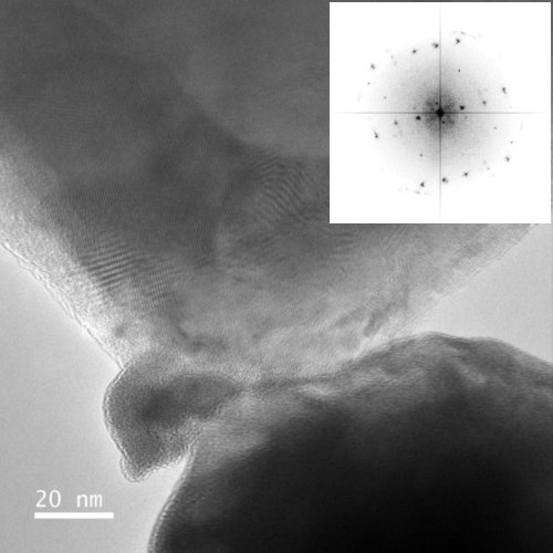
The example shows a TEM image of a 60 nm-wide contact between the mobile biasing probe and a metal-based sample. The structure of the contact has been resolved with high spatial resolution.