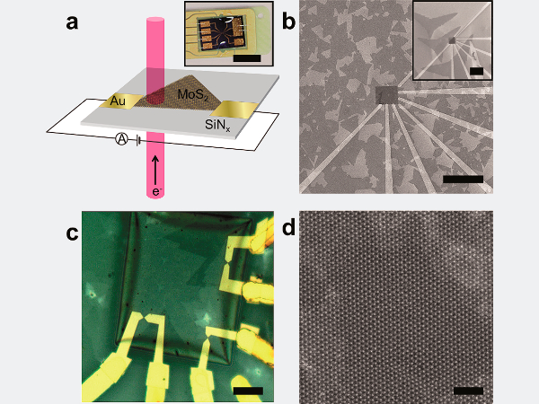
Two-dimensional materials-based electronic devices are particularly well suited for in-situ microscopy studies. Is relatively easy to contact continuous films and large crystals of 2D materials with Hummingbird Scientific’s biasing platforms. The example shown here illustrates that 2D materials-based devices suited for TEM studies can also be studied with other characterization techniques, in a correlative manner. Dr. Marija Drndić’s group at the University of Pennsylvania developed a process to study the effects of electron beam irradiation on one-atom-thick MoS2 crystals by combining in-situ TEM and ex-situ Raman spectroscopy data—from the same sample.
Reference: William M. Parkin et al. Raman Shifts in Electron-Irradiated Monolayer MoS2. ACS Nano (2016).
Image © 2014 American Chemical Society

