How can electron holography be used to map electric fields in nanodevices?
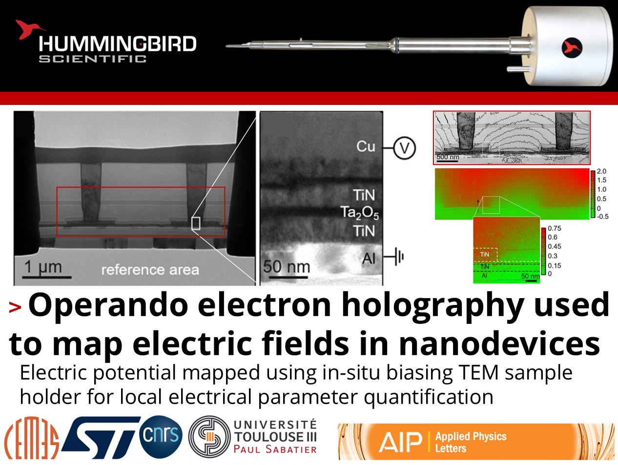
Maria Brodovoi, Cristophe Gatel, and their colleagues at CEMES-CNRS, STMicroelectronics, and University Toulouse III–Paul Sabatier used the Hummingbird Scientific in-situ electrical biasing sample holder to characterize functioning nanodevices using operando electron holography. Metal-insulator-metal (MIM) nanocapacitors were biased under in situ TEM and the electric fields were quantitatively mapped and compared with finite element method modeling to determine local electrical parameters.

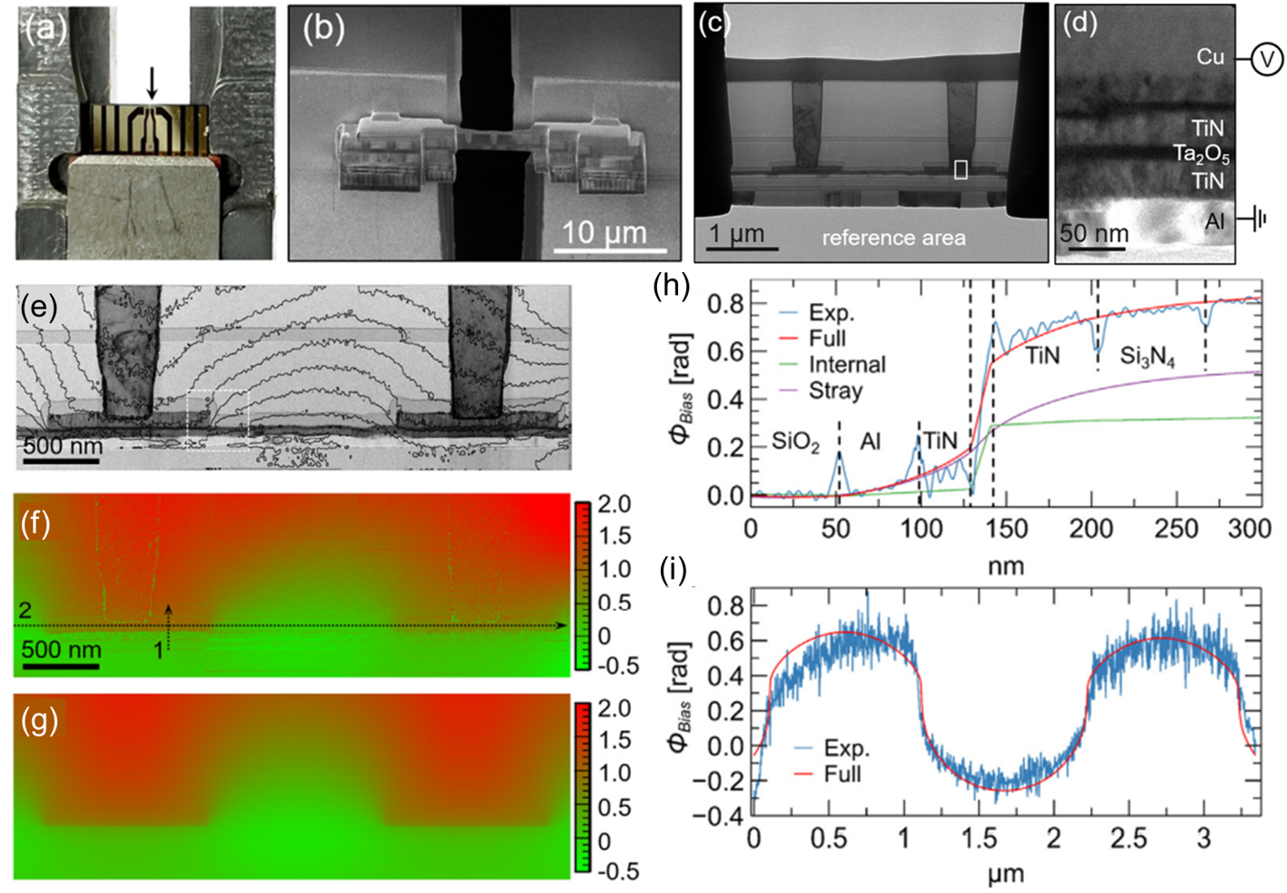
MIM nanocapacitor specimen-device: a) Chip inserted in a sample holder (arrow indicates sample position); b) SEM image of the sample device connected to gold electrodes on chip; c) TEM image of final specimen-device active area; d) enlargement of the MIM nanocapacitor showing stack. Operando electron holography: e) Experimental amplitude image of both MIM nanocapacitors in parallel; f) experimental phase image; g) FEM simulated phase image; h) experimental phase profiles across active layer (black arrow 1) with corresponding simulated profiles for the internal field (green), stray field (purple), and total contribution (red); and i) horizontal phase profiles (black dotted arrow 2). Copyright © 2022 AIP Publishing LLC
Electron-transparent sections of nanodevices were prepared by focused-ion beam (FIB) and affixed to FIB-compatible biasing chips, with the device section bridging two gold electrical leads. In the active area, experimental amplitude and phase mappings were acquired at various applied voltages. Isophase contours presented a sharp variation across different layers of the device, due to strong local electric field in the Ta2O5 dielectric and geometry of the TiN electrodes. COMSOL modeling agreed well with experimental results, allowing local electrical parameters such as the dielectric electrostatic potential, capacitance, and surface charge density to be reliably extracted from the model. The methodology developed for the flexible biasing carrier TEM holder can be applied to more complex nanodevices in the future, for better understanding of the relationship between their chemical, structural, and electrical properties.
Reference:
Maria Brodovoi, Kilian Gruel, Aurélien Masseboeuf, Lucas Chapuis; Martin Hÿtch, Frédéric Lorut, Christophe Gatel, Appl. Phys. Lett., 120 233501 (2022) DOI: 10.1063/5.0092019
Full paper Copyright © 2022 AIP Publishing LLC
View All News

