
Can local electrical resistivity be mapped at the nanoscale?
Leifeng Zhang, Christophe Gatel, and their colleagues at the CEMES-CNRS and STMicroelectronics published recent work using the Hummingbird Scientific in-situ electrical biasing sample holder in combination with operando electron holography performed on a Hitachi HF3300-C TEM to map resistivity changes of phase-change materials in pulse code modulation (PCM) devices. The experimental measurements were supplemented by finite element modeling (FEM) simulations of the prepared devices.
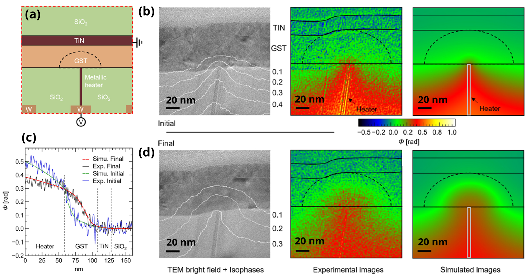
a) Schematic of PCM device showing configuration, corresponds to electron microscopy/holography. b) Bright-field TEM (left), extracted experimental (middle), and simulated (right) phase maps of the initial state. c) Comparison of phase profiles for experimental and simulated phase profiles for the initial (crystalline) and final (amorphous) states. d) Bright-field TEM (left), extracted experimental (middle), and simulated (right) phase maps of the final. Copyright 2024 American Chemical Society
The operando biasing experiments yielded high-resolution electron holograms before and after switching on the PCM device, from which the phase information and local electrical potential were extracted. The local resistivity derived through the FEM, revealed unexpected inhomogeneities near the heated region of the device. The combination of operando biasing hardware and electron interferometry capabilities resulted in a powerful tool for understanding the complex interplay between microstructure, chemistry, and electrical properties in nanoscale devices, and will accelerate the development of memory technologies for the next generation of nanoelectronics.
Reference:
Leifeng Zhang, Frédéric Lorut, Kilian Gruel, Martin J. Hÿtch, and Christophe Gatel, Nano Letters 24 (19) 5913–5919 (2024) DOI: 10.1021/acs.nanolett.4c01462
Full paper Copyright © 2024 American Chemical Society
View All News