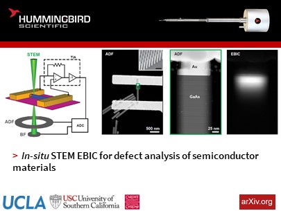
Electronic devices are sensitive to defects but locating them is extremely difficult. Now, researchers from the University of California, Los Angeles, University of Southern California, and Cardiff University have used in-situ scanning transmission electron microscope electron-beam induced current (STEM EBIC) imaging to locate electrically active defects (electron-hole pairs) in the gold (Au) – gallium arsenide (GaAs) nanowire heterojunction device. The work was performed using Hummingbird electrical biasing TEM holder and published in the online arXiv.org.
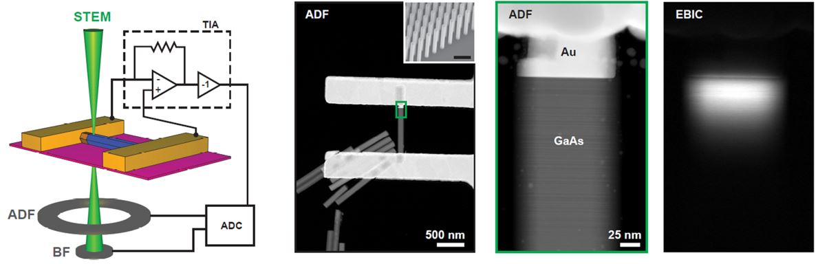
The EBIC image clearly demonstrates the electron-hole pair separation near the Au-GaAs heterojunction (see Figure below). The researchers evaluated different acceleration voltage of TEM and determined that imaging performed at 80kV or 200kV are less damaging, compared to 300kV. The optimal imaging conditions at 80kV and 200kV allowed them to observed decreasing minority charge carrier diffusion along the surface, suggesting the device’s charge collection efficiency (CCE) is limited by surface defects. The technique demonstrated here is a powerful method to study defects in semiconductors at high spatial resolution.
Reference: Brian Zutter, Hyunseok Kim, William Hubbard, Dingkun Ren, Matthew Mecklenburg, Diana Huffaker, and B. C. Regan. Mapping Charge Recombination and the Effect of Point Defect Insertion in Gallium Arsenide Nanowire Heterojunctions. arXiv:2010.05140 (2020). Full paper
View All News