
How can the electrical biasing TEM sample holder be used to measure electronic transport properties at the nanoscale in real-time?
Julio A. Rodríguez-Manzo, A. T. Charlie Johnson, Marija Drndić, and their colleagues at the University of Pennsylvania published on their use of the Hummingbird Scientific in-situ electrical biasing TEM sample holder for electronic transport measurements on graphene nanoribbons (GNRs) in a three-electrode geometry.
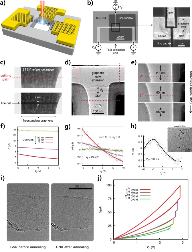
In situ fabrication and electrical characterization of graphene nanoribbon (GNR) devices. a) Schematic of a three-terminal device with a GNR suspended between source and drain electrodes and a nearby graphene side gate. b) SEM image of a three-electrode chip with an electron-transparent SiNx window and a zoomed-in view showing a graphene strip contacting all electrodes. c) Sequential STEM images of the nanosculpting process defining GNRs and side-gate extensions from continuous graphene. d) TEM image of a GNR near a side-gate extension with ~80 nm gate-channel separation. e) Stepwise width reduction of a GNR using electron-beam sculpting with precision. f) Conductance (G) and g) ΔG = G − G0 as a function of Vg for GNRs of different widths. h) Conductance of a graphene constriction versus Vg, with an inset TEM image of the constriction. i) TEM images showing GNR changes before and after in-situ annealing via joule heating. j) I-V characteristics for four annealing cycles showing resistance decrease with increasing Vb.
Graphene was synthesized using atmospheric pressure chemical vapor deposition (CVD) on copper foil and transferred onto TEM-compatible chips featuring electron-transparent SiNx windows and pre-patterned metal electrodes. Freestanding graphene regions were created by etching nanoscale gaps in the SiNx with a focused ion beam. Inside the TEM, a focused electron beam in scanning mode (STEM) was used to precisely sculpt graphene into nanoribbons (GNRs) and adjacent side-gate structures. In situ electrical transport measurements were performed on GNRs of three different widths, revealing that conductance modulation by the side gate became more pronounced as ribbon width decreased—emphasizing the importance of nanoscale dimensions for effective gate control in FET configurations. Numerical simulations confirmed that the graphene-based side-gate extensions significantly enhanced the electric field at the GNR channel, supporting the observed electrical behavior. The Hummingbird Scientific in-situ electrical biasing TEM sample holder enabled seamless integration of fabricated devices allowing for atomic-scale imaging and electrical testing.
Reference: Julio A. Rodríguez-Manzo, Zhengqing John Qi, Alexander Crook, Jae-Hyuk Ahn, A. T. Charlie Johnson, and Marija Drndic, ACS Nano 10, 4 (2016). DOI: 10.1021/acsnano.6b01419
Full paper Copyright © 2016 American Chemical Society
View All News