How does image-based strain measurement compare to conventional TEM nanomechanical techniques?
Sandra Stangebye, Olivier Pierron, and their colleagues at Georgia University of Technology used the Hummingbird Scientific in-situ electrical biasing sample holder to compare in-situ MEMS strain measurements from image-based and capacitive sensing-based techniques. In both techniques, the biasing capability of the holder was used to actuate the tensile deformations of 100-nm thick Au thin film specimens.

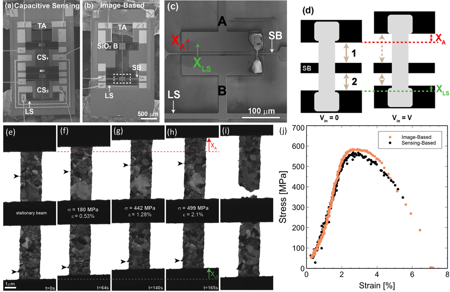
a) Chip layout for capacitive sensing nanomechanical testing device. b) Chip layout for image-based sensing nanomechanical device. The thermal actuator (TA), and load sensor beams (LS) are common to both. c) Zoomed-in view of specimen mounted onto image-based nanomechanical device. d) Schematic of the image-based MEMS operation. e-i) Time-lapse images of in situ monotonic tensile test using the image-based MEMS technique. j) Comparison of electrical- and image-based sensing results under monotonic loading conditions for a UFG Au specimen. Copyright © 2023 Elsevier B.V. All rights reserved.
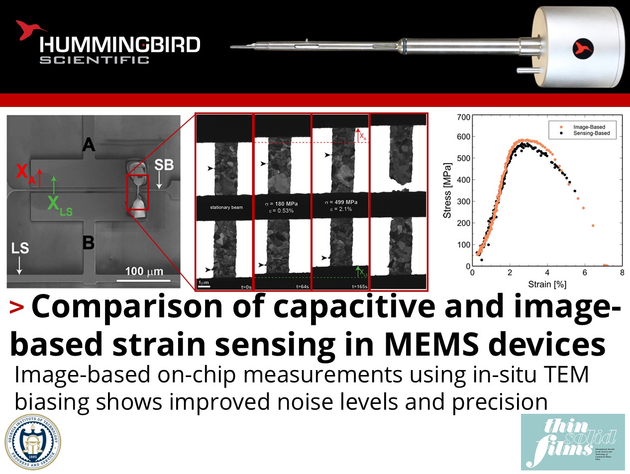
In the capacitive sensing technique, the biasing capability of the holder is also used to measure strain by electrical sensing. In the image-based technique, digital image correlation (DIC) was used to measure local strain by tracking edge features in situ. Overall, the image-based technique yielded a significant improvement in the noise levels from ~1–2 MPa to ~0.2 MPa and increased sensitivity with the capability of measuring small stress changes. Monotonic and transient testing are both possible with the demonstrated novel technique for characterizing the plastic deformation mechanisms of thin films.
Reference: Sandra Stangebye, Xing Liu, Lina Daza Llanos, Yichen Yang, Ting Zhu, Josh Kacher, Olivier Pierron, Thin Solid Films, 787 140125 (2023) DOI: 10.1016/j.tsf.2023.140125
Full paper Copyright © 2023 Elsevier B.V. All rights reserved.
View All News

