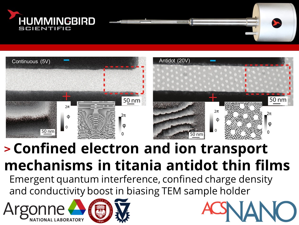
How does nanoscale confinement affect charge transport in oxide films?
Frank Barrows, Amanda Petford-Long, and their colleagues at Argonne National Laboratory, IIT, and University of Chicago used the Hummingbird Scientific in-situ electrical biasing sample holder to explore the effect of nanoscale confinement on charge transport in titania films patterned with an antidot lattice featuring 11-20 nm structures. In-situ electron holography and impedance spectroscopy, complemented by modeling, were applied to characterize these charge transport behaviors.
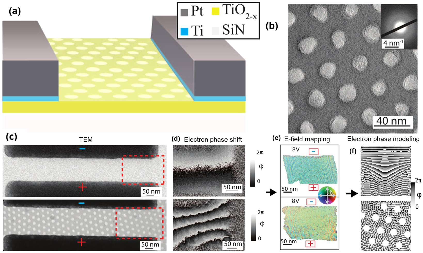
a) Cross-section schematic of the electrode and film layers. The bilayer electrodes (1.5 nm Ti/110 nm Pt) have a width of 1 μm and a gap of 180 nm. b) TEM image of a titania film patterned into an antidot array. The dark regions are the titania film, and the bright regions are the voids, which form a hexagonal array. An electron diffraction pattern of the amorphous titania is inset. c) TEM images of continuous (upper) and antidot (lower) titania films, respectively, with positive and negative electrodes indicated. Electron holography data obtained from region highlighted with a red box. d) Reconstructed electron phase shift for regions corresponds to the boxes in (c). e) Color vector maps of the electric field, F̂, in a continuous (upper) and antidot (lower) film for an applied bias of 8 V. The direction of F̂is indicated by the color wheel. f) c) Maps of electron wave function phase (φ) in the continuous (upper) and antidot (lower) films at 0.3 eV at 0.2 V applied bias (gray). Copyright © 2021 UChicago Argonne, LLC, Operator of Argonne National Laboratory. Published by American Chemical Society
Under voltage applied by the Hummingbird holder, a shift in transport mechanisms from ion and vacancy motion to electron hopping is observed when nanoscale confinement is introduced. The patterned films exhibited unique properties, including the absence of hysteresis and filamentation typically seen in continuous films. Instead, they demonstrated anomalous conductivity attributed to room temperature quantum interference – a novel observation in quantum-confined systems. By suppressing ion and vacancy transport, the nanoscale patterning prevents microstructural changes under applied bias and eliminates volatile hysteresis in current-voltage characteristics. The work gives insight into the interplay between confined charge density and displacement fields in spatially confined thin films, with implications for resistive switching and photocatalytic applications in metal oxides.
Reference:
Frank Barrows, Hanu Arava, Chun Zhou, Paul Nealey, Tamar Segal-Peretz, Yuzi Liu, Saidur Bakaul, Charudatta Phatak, Amanda Petford-Long, ACS Nano, 15 (8) 12935–12944 (2021) DOI: 10.1021/acsnano.1c01340
Full paper Copyright © 2021 UChicago Argonne, LLC, Operator of Argonne National Laboratory. Published by American Chemical Society
View All News