Electron beam-induced current (EBIC) imaging of DB in Pt/HfO2/Ti valence change memory devices
William A. Hubbard at NEI and team from the Regan Research Group at UCLA used in situ scanning transmission electron microscopy (STEM) electron beam-induced current (EBIC) to visualize the electronic signatures of Dielectric Breakdown.
They used Hummingbird Scientific’s Electrical Biasing TEM holder to visualize these electronic signatures.

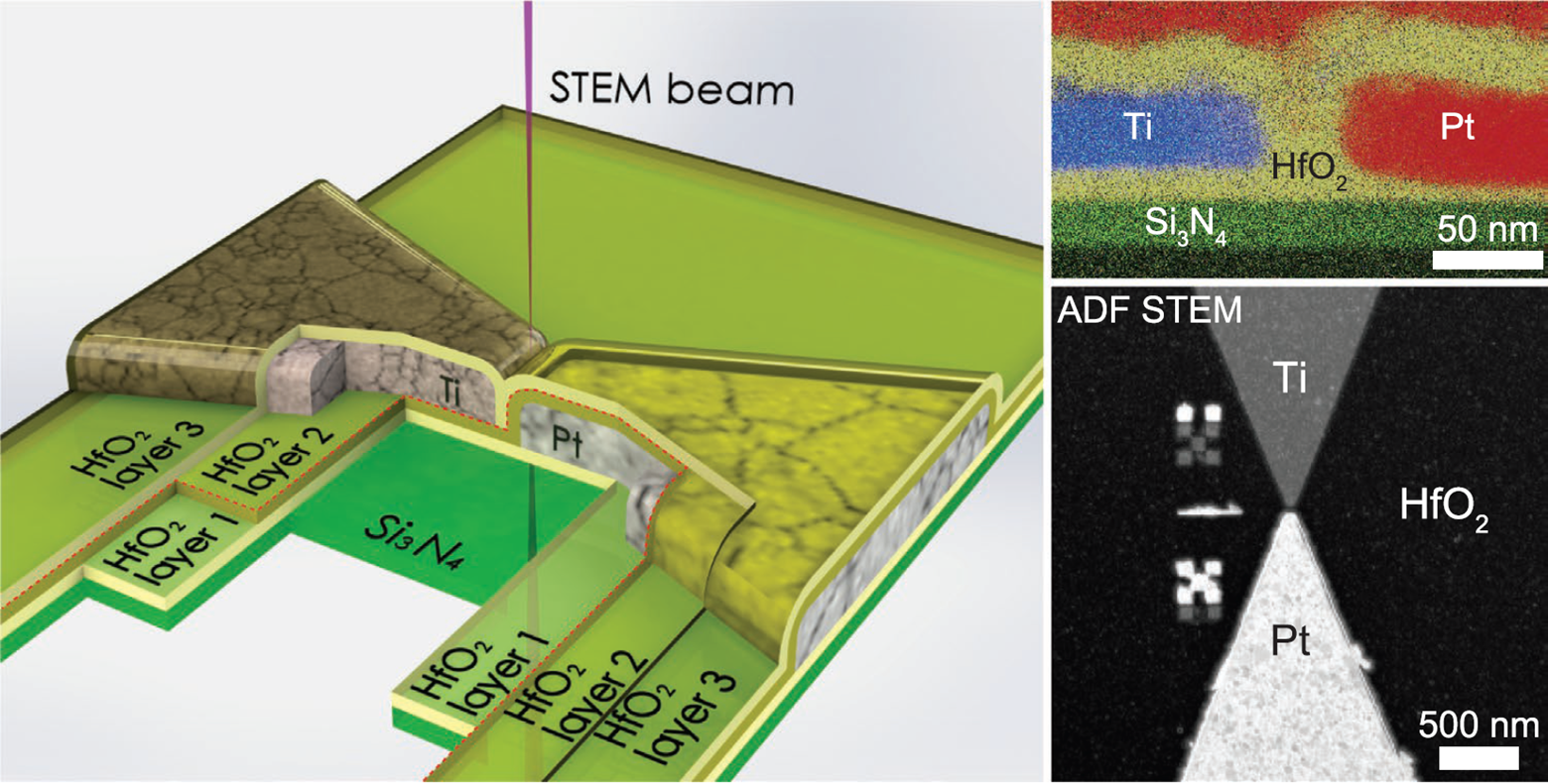
Figure 1. Valence Change Memory (VCM) slant-vertical device architecture. (left) A VCM device, shown entirely to-scale with cutaways (Right top) X-ray energy dispersive spectroscopy (EDS) data (Right bottom) Low magnification ADF STEM shows a slant-vertical device in plan-view. Copyright © 2022 Advanced Functional Materials
Reference: William A. Hubbard, Jared J. Lodico, Ho Leung Chan, Matthew Mecklenburg, Brian C. Regan “Imaging Dielectric Breakdown in Valence Change Memory” Copyright © 2022 Advanced Functional Materials. Full Paper
View All News

