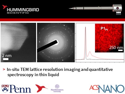
Recently, we collaborated with researchers at the University of Pennsylvania and Northwestern University and published a technique demonstrating in-situ atomic-scale imaging in the environmental liquid cell transmission electron microscopy (TEM) using Hummingbird Scientific’s TEM liquid cell electrochemistry system. We also show methods to perform quantitative structural and chemical analysis using Selected Area Electron Diffraction (SAED) and Electron Energy Loss Spectroscopy (EELS) by creating a thin layer of liquid around the sample, respectively. Details about the methodology and example images have been published in the journal, ACS Nano.
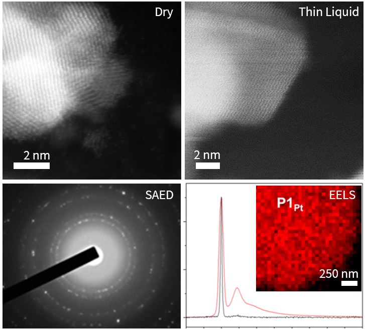
The work demonstrates that the thickness of the liquid layer around the sample can be reduced by systematically performing water splitting in-situ to generate a gas bubble. The bubble allows controlling the liquid layer thickness to around 30 nm film layer. The reduced thickness in the liquid layer then allows the acquisition of atomic-scale scanning TEM (S/TEM) images with chemical analysis using EELS and structural analysis through SAED. The technique presented here can be broadly used in other multimodal characterization tools to understand nanoscale solid-liquid interfaces.
Reference: Rui Serra-Maia, Pawan Kumar, Andrew C. Meng, Alexandre C. Foucher, Yijin Kang, Khim Karki, Deep Jariwala, Eric A. Stach. ” Nanoscale Chemical and Structural Analysis during In Situ Scanning/Transmission Electron Microscopy in Liquids,” ACS Nano (2021). Full Paper
View All News